Screen printing processes in the semiconductor industry
The use of screen printing processes in the semiconductor industry is a recent innovation. Progressive semiconductor manufacturers now use screen printing for a variety of advanced materials applications at wafer level and final package assembly.Why Choose a DEK Precision Screen?
Semiconductor manufacturers keen to reduce manufacturing costs embrace the benefits of employing cost-effective, advanced screen printing technology for processes as diverse as solder bumping and die attach. DEK precision screens and stencil are meticulously designed to meet the unique challenges of semiconductor applications.
Emulsion thickness 0 - 50µm ± 2µm; 51 - 100µm ± 5µm; 101 - 500 µm ±10%; 501 - 1000µm ±15%
Line widths from 50µm
Maximum Frame size 1000 x 1000mm O/D
Produced in clean room facilities constructed to FED STD 209E Class 10,000 (BS EN ISO 14644-1 Class 7)
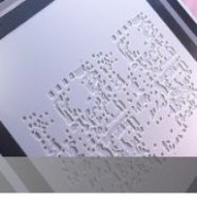
Ball Placement (Stencil) Accuracy; every DEK precision stencil deployed in ball placement semiconductor applications is chemically etched or electroformed to a tolerance of a few microns. Each process can produce up to 800,000 apertures. Automated inspection is engaged during manufacture to ensure that every aperture meets the diametric and positional specifications for the application
Increased Throughput; the direct imaging capability of stencil deployed in ball placement ensures that solder bumping balls are placed quickly and precisely. This delivers a substantial increase in placement speed over traditional vacuum placement methods
Cost Effectiveness; the price of a fully-inspected stencil placement tool is highly cost-competitive with alternative process options
Manufacturing Repeatability; our new clean room manufacturing facility, constructed to FED STD 209E Class 10,000 (BS EN ISO 14644-1 Class 7), ensures process integrity from our production environment to your factory
Product Matched to Process; DEK’s applications support team uses our proprietary stencil tool design calculator to ensure that we recommend to you the optimum screen and stencil characteristics based on the solder ball size used in your process
Visit the DEK Printing Machines Ltd website for more information on Screen printing processes in the semiconductor industry


