Applied Thin-Film Products - Capabilities Overview
ATP makes its own hard surface photomasks in a Class-100 chamber, produced on precision pattern-generated equipment. ATP routinely produces images in chrome and iron oxide on high-quality soda lime glass, and has extensive expertise in imaging on photographic emulsion. Masks are typically generated from AutoCAD, DWG or DXF files, and SolidWorks.Sputtering is the deposition method of choice due to its superior adhesion. The basic metalisation scheme for thin film substrates contains TiW as the adhesion layer and Au as the conductor layer (TiW/Au). Solderable metalisation is achieved by adding Ni and / or Cu. Palladium can also be added as a solderable film when using high temperature eutectic solders such as the SAC products. The final combination depends on the customer application.
TaN resistor metalisation can be integrated onto substrates to allow for a wide range of resistivities - 10-200 ?/Sq. The most cost-effective ones are 50, 75 & 100 ?/sq. Resistor tolerances are dependant on material surface finishes and resistor design layout. ATP also offers laser trimming to tolerances as low as �0.5%, or �0.25 ?, if required.
Computer-controlled lasers at ATP can create features of virtually any planar shape in ceramic substrates, and can deliver a positional accuracy of 0.001? (0.0254mm) or better over areas as large as 8?x8? (203.2mm x 203.2mm). The lasers are extremely flexible and permit close location of features with considerable layout flexibility. These shapes include circles, curves, rectangles, polygons, rounded thin slots, etc.
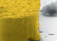
Ion Beam Milling is a dry etching technique where the ions of an inert gas are accelerated from an ion source into the surface of the substrate in order to remove metals, providing an alternative to traditional wet etching methods. Because it is an anisotropic process, metal removal only occurs in the Z-axis, resulting in minimum undercutting of the underlying metals during the removal process, and achieving nearly-vertical sidewall profiles repeatedly.
12345PreviousNext
ATP Capabilities Downloads
File
Photomask Requirements
Download
File
CAD Data Guidelines
Download
File
Standard Metalisation Schemes
Download
File
Integrated TaN Resistor Information
Download
File
Laser Machining & Drilling
Download
File
Ion Beam Milling
Download
Visit the Inseto (UK) Ltd website for more information on Applied Thin-Film Products - Capabilities Overview

