Optoelectronic and Photonic Wafer Probe Equipment
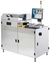
Key FeaturesOpto-electronic Wafer Probe EquipmentWafer level test: LED's, VCSEL's and Silicon Photonic devices etc.Integration of Integrating Spheres and Fibre AlignmentManual, Semi and Fully Automatic ConfigurationsTest individual die, partial wafer through 300 mm wafersSingle and Double sided probe test Test hot or cold with chucks, LEC's or thermal streams etc.
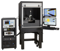
SemiProbe has pioneered new electro-optical methods and capabilities for testing optoelectronic and photonic components at wafer level and has extensive experience testing silicon photonic devices and compound materials, including light emitting diodes (LED), vertical cavity surface emitting lasers (VCSEL) and photo diodes etc.
Their unique integrating sphere holder enables users to utilize the same PS4L system for horizontal (EELD) and vertical (VCSEL, LED) testing in either a manual or semiautomatic configuration. SemiProbe have created wafer maps capable of mapping >100k die, unique chuck systems to handle fragile or broken wafers, high speed stages and software to increase throughput.
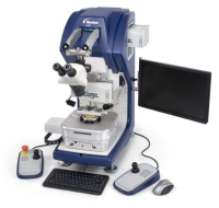
Further developments also include manual, semi and fully double side probing (DSP) capability, which allows the user the flexibility to probe from the top and bottom sides. In some cases an emission microscope or a solar simulator will be mounted on one side and the other side would be the bias or electrical stimulation side. The DSP has both topside and bottom-side optics that provides the ability to view both sides independently or at the same side.
In addition, capabilities include sub-micron fibre alignment for testing of silicon photonic devices using manual or automated multi-axis positioners and laser measurement for continuous adjustment of wafer planarity.
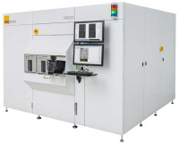
Manual, semi and fully automated electro-optical systemsMultiple applications: SSP, DSP, Vacuum, HF, OPTO & moreLight measurements via Fibre or Integrating Sphere etc.Test single die, laser bars, partial or full wafer up to 300 mmExtensive range of options and featuresLow cost and field upgradeable
12345678910PreviousNext
Optoelectronic and Photonic Wafer Probe Downloads
File
Optoelectronic Probing System Overview
Download
File
VCSEL Solutions Overview
Download
File
SemiProbe Corporate Overview Datasheet
Download
Visit the Inseto (UK) Ltd website for more information on Optoelectronic and Photonic Wafer Probe Equipment
ENQUIRY FORM