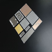
Direct Bond Copper
Product Code: None
DBC means Direct Bonded Copper and denotes a process in which copper and a ceramic material are directly bonded. Direct bonded copper substrates have been proven for many years as an excellent solution for electrical isolation and thermal management of high power semiconductor modules. The advantages of DBC substrates are high current carrying capability due to thick copper metallization and a thermal expansion close to the silicon at the copper surface due to high bond strength of copper to ceramic.Normally, DBC has two layers of copper that are directly bonded onto an aluminum-oxide (Al2O3) or aluminum-nitride (AlN) ceramic base. The DBC process yields a super-thin base and eliminates the need for the thick, heavy copper bases that were used prior to this process. Because power modules with DBC bases have fewer layers, they have much lower thermal resistance values. And because the expansion coefficient matches silicon, they have much better power cycling capabilities (up to 50,000 cycles).
Disadvantage of DBC(Direct Bonded Copper)
The drawback of standard DBC substrates for high voltage applications is a start of partial discharge at relatively low voltages. Therefore another kind of substrates using expensive metal brazing technologies is mainly used in high voltage semiconductor modules for traction applications. The initiation voltage for ceramic thickness of 0.63mm is less than 4 kV. Main causes for this behavior are small voids between copper and ceramic and blurred straight border lines of the copper conductors at the copper/ceramic interface. The new DBC process and an improved etching technology are eliminating these disadvantages. The other disadvantage of DBC is its deficiency for thermal shock because of the very large residual stress on the substrate surface due to the CTE mismatch of alumina and copper.
Properties of DBC ceramic substrates:
Good mechanical strength; mechanically stable shape, good adhesion and corrosion resistant
Excellent electrical insulation
Very good thermal conductivity
Superb thermal cycling stability
The thermal expansion coefficient is close to that of silicon, so no interface layers are required
Good heat spreading
May be structured just like printed circuit boards or "IMS substrates"
Environmentally clean
Direct Bonded Copper
Advantages to the user:
The 0.3 mm thick copper layer permits higher current loading for the same conductor width. Assuming the same copper cross-section, the conductor needs to be only 12% of that of a normal printed circuit board
Excellent thermal conductivity provides the possibility of very close packaging of the chips. This translates into more power per unit of volume and improved reliability of systems and equipment
The high insulation voltage allows the use of thin dielectric material (alumina) for improved thermal dissipation for high voltage applications.
DBC ceramic is the basis for the "chip-on-board" technology which represents the packaging trend for the future
DBC ceramic substrates are the base materials of the future for both the construction and the interconnection techniques of electronic circuits. Therefore DBC is used in our daily environment, such as:
Power hybrids and power control circuits
Power semiconductor modules
Smartpower building blocks
Solid state relays
High frequency switch mode power supplies (SMPS)
Electronic heating devices
Building blocks for automobile electronics, as well as aerospace technology
The newly developed DBC technologies of the liquid cooled and the partial discharge free substrates have a great potential to expand further application fields of DBC substrates as well as high power semiconductor modules in the near future.
Visit the ELE Advanced Ceramics website for more information on Direct Bond Copper


